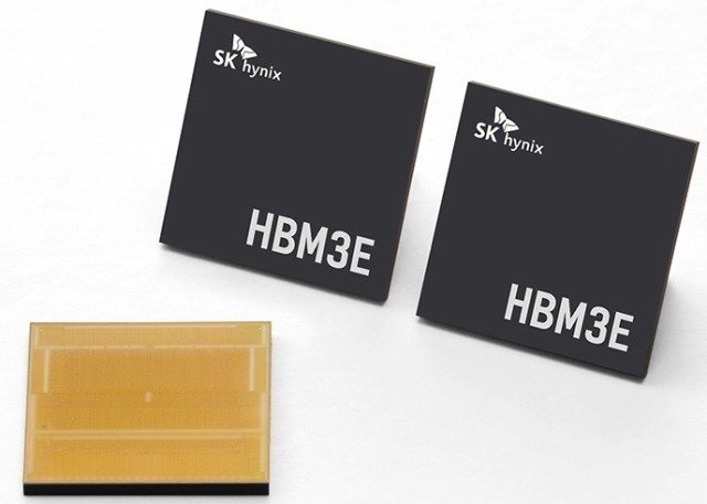
SK Hynix, a leading semiconductor manufacturer, has commenced the mass production of HBM3E, the latest advancement in AI memory technology, for delivery to a customer starting from late March.

The company’s achievement in HBM3E development, announced just seven months ago, marks a significant milestone in the realm of ultra-high-performance memory solutions.
HBM (High Bandwidth Memory), renowned for its vertically interconnected DRAM chips, stands out for its superior data processing speed compared to conventional DRAM products. HBM3E, the latest iteration in this series and the fifth generation overall, builds upon this legacy of innovation established by HBM, HBM2, HBM2E, and HBM3.
As the inaugural provider of HBM3E, featuring top-performing DRAM chips, SK Hynix extends its track record of success following the introduction of HBM3. The company anticipates that the successful volume production of HBM3E, coupled with its pioneering role in offering HBM3, will solidify its position as a leader in the AI memory domain.
In today’s AI-driven landscape, where rapid data processing is imperative, the composition of semiconductor packages plays a crucial role. Major global tech firms increasingly demand enhanced performance from AI semiconductors, and SK Hynix positions its HBM3E as the optimal solution to meet these escalating requirements.
Distinguished as the industry’s foremost AI memory product, HBM3E excels across all essential parameters, including speed and heat management. With the capacity to process up to 1.18TB of data per second, equivalent to over 230 full-HD movies in a single second, it sets a new benchmark for efficiency and performance.
Moreover, given the high-speed operation inherent to AI memory, effective heat control is paramount. SK Hynix’s HBM3E boasts a 10 percent improvement in heat-dissipation performance compared to its predecessor, thanks to the integration of the advanced MR-MUF (Mass Reflow Molded Underfill) process.
MR-MUF, a critical aspect of SK Hynix’s advanced technology, involves stacking semiconductor chips and injecting liquid protective materials between them to enhance heat dissipation and ensure circuit protection. This innovative approach significantly improves heat dissipation efficiency compared to conventional methods, contributing to stable mass production within the HBM ecosystem.
Sungsoo Ryu, Head of HBM Business at SK Hynix, expressed confidence in the company’s comprehensive lineup of AI memory solutions with the completion of HBM3E mass production.
HBM capacity of SK Hynix is around 120K, though capacity may vary based on validation progress and customer orders.
Regarding market share for current mainstream HBM3 products, SK Hynix holds over 90 percent of the HBM3 market, while Samsung is expected to closely follow with the gradual release of AMD’s MI300 over the next few quarters, TrendForce says.
Samsung’s total HBM capacity is expected to reach around 130K (including TSV) by year-end, according to TrendForce.
Baburajan Kizhakedath
