
A recent investigation by TrendForce into the aftermath of a powerful earthquake in the Noto region of Ishikawa Prefecture, Japan, has highlighted potential impacts on crucial semiconductor-related facilities situated within the affected area.
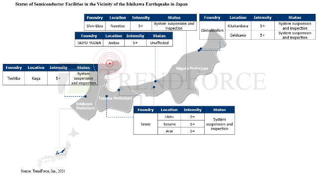 Key players, including MLCC manufacturer TAIYO YUDEN, silicon wafer producers Shin-Etsu and GlobalWafers, as well as Toshiba and TPSCo (a joint venture between Tower and Nuvoton), find themselves within the quake-affected zone.
Despite concerns stemming from the semiconductor industry’s ongoing slowdown and the off-peak season, preliminary assessments following the earthquake suggest that the majority of these facilities remain within the structural tolerance levels suitable for seismic activity.
The report said existing component inventories coupled with the location of most factories in areas with seismic intensities of level 4 to 5 have contributed to initial reports indicating manageable impacts and no significant damage to machinery.
Of particular note are the silicon wafer production facilities of Shin-Etsu and GlobalWafers in Niigata, currently undergoing shutdowns for inspections due to the sensitivity of the crystal growth process in raw wafer manufacturing.
However, Shin-Etsu’s primary crystal growth operations in the Fukushima area have limited exposure to the quake’s effects, minimizing potential disruptions. SUMCO, another player in this arena, has reported no adverse effects.
Turning to the semiconductor sector, Toshiba’s Kaga facility in Ishikawa Prefecture’s southwestern region, encompassing six-inch, eight-inch, and a recently constructed twelve-inch facility, is undergoing thorough inspections.
Simultaneously, TPSCo’s factories in Uozu, Tonami, and Arai—established through a collaboration between Tower and Nuvoton — are also temporarily shut down for assessments. Notably, USJC, which is UMC’s acquisition of the Mie Fujitsu plant area in 2019, remained unaffected.
On a positive note, TAIYO YUDEN’s new Niigata plant, designed to withstand seismic activity up to level 7, reported no equipment damage. Additionally, while Murata and TDK’s MLCC plants experienced seismic intensities below level 4 and remained largely unaffected, Murata’s other non-production MLCC factories in Komatsu, Kanazawa, and Toyoma — areas with seismic intensities above 5 — are currently closed for the New Year holiday, with staff assessing any potential damage.
As the semiconductor industry navigates through this seismic event, initial reports suggest a resilient infrastructure and proactive measures in place to manage the impact, minimizing disruptions to critical production processes.