

Global spending on 300mm front-end semiconductor fab equipment is projected to reach $149 billion in 2026, up 31 percent year-on-year, according to SEMI. Investment is expected to maintain double-digit annual growth through 2029, when spending is forecast to reach $227 billion.

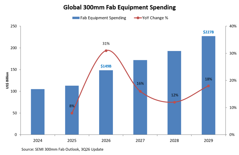
The outlook signals a sustained expansion in semiconductor manufacturing capacity for artificial intelligence, high-performance computing, memory and other chip applications. For equipment vendors, the opportunity spans lithography, deposition, etching, wafer cleaning and process control.
SEMI’s latest 300mm Fab Outlook also identifies a substantial pipeline of new factories and production lines, supporting equipment demand beyond the current investment cycle.
Semiconductor Equipment Investment to Rise by $78 Billion
The increase from $149 billion in 2026 to $227 billion in 2029 represents $78 billion in additional annual equipment spending, or approximately 52 percent growth over the period.
These figures cover equipment investment in front-end 300mm facilities, where semiconductor devices are manufactured on wafers. They should be distinguished from fab construction expenditure and spending on chip assembly, packaging and testing.
The expansion creates opportunities across several manufacturing stages. Advanced logic requires increasingly precise transistor and interconnect processing, while more complex memory structures require deeper etching and tighter control over deposited materials.
38 New Fabs and Production Lines to Start Construction
Excluding facilities dedicated solely to research and development, SEMI projects 20 new 300mm fabs or production lines to begin construction worldwide in 2026, followed by 18 in 2027.
The United States is expected to account for three construction starts in 2026 and four in 2027.
Across all 300mm facilities, global fab construction spending is forecast to increase 23 percent to $47.5 billion in 2026, followed by another 33 percent increase to $63.3 billion in 2027. Expenditure is projected to reach $68.4 billion in 2028.
Construction starts and equipment purchases occur at different stages of a fab project. The expanding building pipeline therefore provides a longer-term indication of potential tool demand, although purchasing schedules depend on individual projects reaching equipment installation and production readiness.
Americas Equipment Spending to More Than Double
Equipment investment in the Americas is projected to rise from $18.1 billion in 2026 to $40.6 billion in 2029.
That represents an increase of approximately 124 percent, reflecting the region’s expanding semiconductor manufacturing footprint.
Globally, SEMI expects 13 new 300mm fabs or lines to begin operations or ship first silicon in 2026, increasing to 23 in 2027. First silicon is an initial production milestone; subsequent output growth depends on process qualification, manufacturing yields and customer requirements.
ASML, Applied Materials and Lam Research Address Critical Processes
ASML supplies extreme ultraviolet and deep ultraviolet lithography systems used to print chip patterns. Its portfolio addresses different layers and manufacturing requirements, making both EUV and DUV relevant to semiconductor capacity expansion. ASML’s TWINSCAN NXT:870B dry lithography system supports 300mm wafers and offers throughput of 400 wafers per hour
Applied Materials supplies deposition, etch, materials modification and other processing technologies. Its gate-all-around transistor technologies address manufacturing steps including epitaxy, selective material removal and electron-beam metrology. In April 2026, the company introduced deposition systems for advanced logic, including the Endura Trillium ALD system for depositing metals in complex transistor gate stacks.
Lam Research addresses memory manufacturing through deposition and etch equipment. Its Lam Cryo 3.0 cryogenic etching technology works with Flex and Vantex platforms used for critical channel-hole etching in high-volume 3D NAND production. This capability is relevant as memory manufacturers build increasingly tall, complex structures.
Tokyo Electron and KLA Support Productivity and Yield
Tokyo Electron supplies coater/developer, deposition, etch and cleaning equipment. Its CLEAN TRACK LITHIUS Pro DICE platform supports 300mm wafers and EUV processing, including High NA. Tokyo Electron says its defect-control technology can reduce defects and associated costs caused by flawed resist coating by at least 50 percent compared with previous models.
KLA supplies inspection, metrology and analytics systems that help manufacturers identify defects and control production processes. Its eSL10 electron-beam inspection system targets defects in complex leading-edge chip structures, helping shorten investigations into yield and reliability problems.
These vendors illustrate where expanding fab budgets can be deployed. SEMI’s forecast does not allocate the projected spending to individual suppliers, and vendor revenue will depend on technology choices, customer orders and project execution.
BABURAJAN KIZHAKEDATH